

GLOBALFOUNDRIES Demonstrates 2.5D High-Bandwidth Memory Solution for Data Center, Networking, and Cloud Applications
Solution leverages 2.5D packaging with low-latency, high-bandwidth memory PHY built on FX-14™ ASIC design system
Santa Clara, Calif., August 9, 2017 – GLOBALFOUNDRIES today announced that it has demonstrated silicon functionality of a 2.5D packaging solution for its high-performance 14nm FinFET FX-14™ integrated design system for application-specific integrated circuits (ASICs).
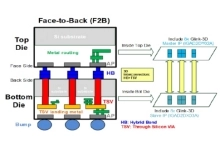
The 2.5D ASIC solution includes a stitched interposer capability to overcome lithography limitations and a two terabits per second (2Tbps) multi-lane HBM2 PHY, developed in partnership with Rambus, Inc. Building on the 14nm FinFET demonstration, the solution will be integrated on the company’s next-generation FX-7™ ASIC design system built on GF’s 7nm FinFET process technology.
“With the tremendous advances in interconnect and packaging technology that has occurred in recent years, the line between wafer processing and packaging has blurred,” said Kevin O’Buckley, vice president of ASIC product development at GF. “Incorporating 2.5D packaging into ASIC design boosts performance beyond scaling and is a natural evolution of our capabilities. It enables us to support our customers in a one-stop end-to-end fashion, from product design all the way through manufacturing and testing.”
The Rambus memory PHY is aimed at high-end networking and data center applications performing the most data-intensive tasks in systems requiring low-latency and high-bandwidth. The PHY is compliant with the JEDEC JESD235 HBM2 standard, supporting data rates up to 2Gbps per data pin, enabling a total bandwidth of 2Tbps.
“We strive to deliver comprehensive HBM PHY technologies that will enable data center and networking solution providers to meet today’s most demanding workloads and take advantage of compelling market opportunities,” said Luc Seraphin, senior vice president and general manager, Memory and Interfaces Division at Rambus. “Our collaboration with GF combines our HBM2 PHY with their 2.5D packaging and FX-14 ASIC design system and provides a fully-integrated solution for the industry’s fastest-growing applications.”
FX-14 and FX-7 are complete ASIC design solutions that take advantage of GF’s experience in volume production with FinFET process technology. They comprise functional modules based on the industry’s broadest and deepest intellectual property (IP) portfolio, which makes possible unique solutions for next-generation wired/5G wireless networking, cloud/data center servers, machine learning/deep neural networks, automotive, and aerospace/defense applications. GF is one of only two companies in the world that delivers best-in-class IP plus advanced memory and packaging solutions.
About GF:
GLOBALFOUNDRIES is a leading full-service semiconductor foundry providing a unique combination of design, development, and fabrication services to some of the world’s most inspired technology companies. With a global manufacturing footprint spanning three continents, GLOBALFOUNDRIES makes possible the technologies and systems that transform industries and give customers the power to shape their markets. GLOBALFOUNDRIES is owned by Mubadala Development Company. For more information, visit http://www.globalfoundries.com.
|
||||||


Related News
- Rambus Announces Silicon-proven R+ DDR4 PHY on GLOBALFOUNDRIES 14nm LPP Process for Networking and Data Center Applications
- Rambus Delivers 112G XSR/USR PHY on TSMC 7nm Process for Chiplets and Co-Packaged Optics in Networking and Data Center
- Rambus and Northwest Logic Certify Interoperability of HBM2 Interface Solution for High-performance Networking and Data Center Applications
- Rambus Advances New Era of Data Center Architecture with CXL Memory Interconnect Initiative
- Cadence Collaborates with STMicroelectronics on Networking, Cloud and Data Center Electronics
Breaking News
- Omni Design Technologies Joins Intel Foundry Accelerator IP Alliance
- Efabless Announces the Release of the OpenLane 2 Development Platform, Transforming Custom Silicon Design Flows
- TSMC Reports First Quarter EPS of NT$8.70
- Brisbane Silicon publishes DPTx 1.4 IP Core
- GUC provides 3DIC ASIC total service package to AI/HPC/Networking customers
Most Popular
- U.S. Subsidy for TSMC Has AI Chips, Tech Leadership in Sight
- Cadence Unveils Palladium Z3 and Protium X3 Systems to Usher in a New Era of Accelerated Verification, Software Development and Digital Twins
- Zhuhai Chuangfeixin: OTP IP Based on 90nm CMOS Image Sensor Process Technology Successfully Mass Production
- Silvaco Announces Expanded Partnership with Micron Technology
- OPENEDGES Unveils ENLIGHT Pro: A High-Performance NPU IP Quadrupling its Previous Generation's Performance
|
|
E-mail This Article |
|
Printer-Friendly Page |